[9 Steps] ‘Design multipurpose UP/DOWN fading LED lights circuit’
Global warming is a serious issue these days and anything that contributes to minimizing global warming should be encouraged. The energy saver bulbs used in the past produced carbon which was dangerous for health. With technology advancement, Light Emitting Diodes (LEDs) were invented and they produced less carbon and hence, contributed to minimizing global warming. The demand for LEDs is increasing rapidly nowadays because they are not much costly and they last longer. In this project, we will make an Up Down Fading LED circuit which could be used domestically as well as commercially. The LED is faded out when it is applied some voltage and at that instant, the charging and discharging of the capacitor occurs. The working principle along with the circuit diagram is mentioned below.
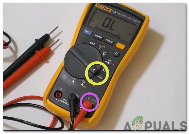
How To Integrate Capacitors And Resistors During Circuit Making?
Now, as we have the basic idea of our project, let’s move towards collecting the components, designing the circuit on software for testing and then finally assembling it on hardware.
Step 1: Components Needed
- No products found.
- 100k Ohm Resistor (x2)
- 10k Ohm Resistor (x1)
- 39k Ohm Resistor (x1)
- 100 Ohm Resistor (x1)
- No products found.
- LED's
- Tacticle Push Button Switch
- Jumper Wires
- No products found.
- Battery Clip
- Printed Circuit Board
- FeCl3
- Soldering Iron
- Hot Glue Gun
Step 2: Components Needed (Software)
- Proteus 8 Professional (Can be downloaded from Here)
After downloading the Proteus 8 Professional, design the circuit on it. We have included software simulations here so that it may be convenient for beginners to design the circuit and make appropriate connections on the hardware.
Step 3: Studying The Components
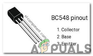
Now as we have made a list of all the components that we are going to use in this project. Let us move a step further and go through a brief study of all the main components. Among all of them, the BC 548 transistor holds significant importance.
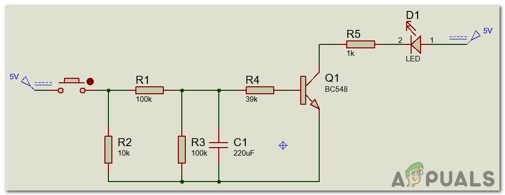
BC 548 NPN Transistor: It is a general-purpose transistor that is used for two main purposes mostly (Switching and amplification). The range of gain value for this transistor is between 100-800. This transistor can handle a maximum current of about 500mA hence it is not used in the type of circuit that has loads that operate on larger amperes. When the transistor is biased it allows current to flow through it and that stage is called saturation region. When the base current is removed transistor is off and it goes in fully Cut-off region.
Step 4: Working Principle Of The Circuit
The main role in the circuit is of two components. (Transistor and Capacitor). LED doesn’t operate in the reverse biased mode, it only operates in the forward-biased mode i.e, When it is connected to the positive terminal of the power supply. The push-button is installed in the circuit and when that push button is pressed and released, the charging and discharging process of the capacitor is started. When the button is pressed the capacitor starts charging and when it is released it starts discharging.
Step 5: Simulating the circuit
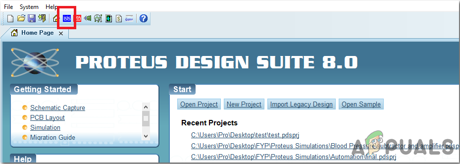
Before making the circuit it is better to simulate and examine all the readings on a software. The software we are going to use is the Proteus Design Suite. Proteus is a software on which electronic circuits are simulated.
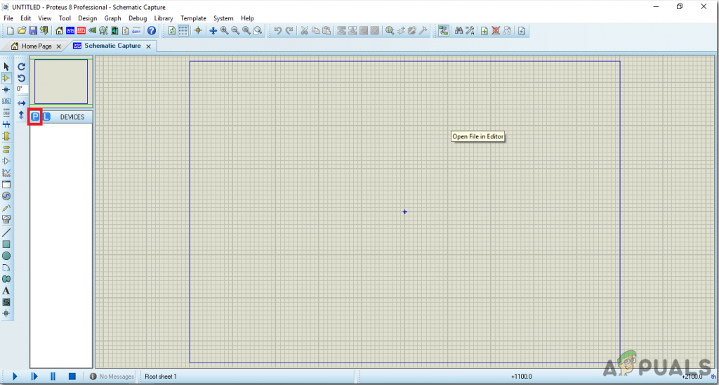
- After you download and install the Proteus software, open it. Open a new schematic by clicking the ISIS icon on the menu.
ISIS - When the new schematic appears, click on the P icon on the side menu. This will open a box in which you can select all the components that will be used.
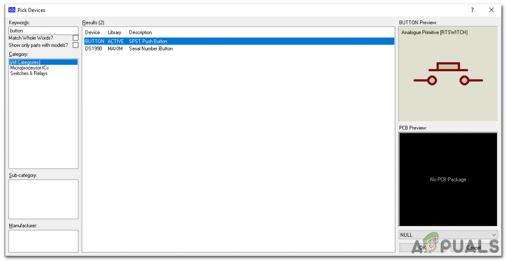
New Schematic - Now type the name of the components that will be used to make the circuit. The component will appear in a list on the right side.
Selecting Components - In the same way, as above, search all the components. They will appear in the Devices List.
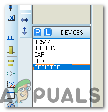
Component List
Step 6: Making a PCB Layout
As we are going to make the hardware circuit on a PCB, We need to make a PCB layout for this circuit first.
- To make the PCB layout on Proteus, we first need to assign the PCB packages to every component on the schematic. to assign packages, right mouse clicks on the component you want to assign the package and select Packaging Tool.
- Click on the ARIES option on the top menu to open a PCB schematic.
- From the Components List, Place all the components on the screen in a design you want your circuit to look like.
- Click on the track mode and connect all the pins that the software is telling you to connect by pointing an arrow.
- When the whole layout is made, it will look like this :
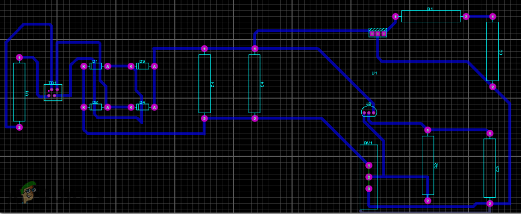
PCB Layout
Step 7: Circuit Diagram
After making the PCB layout the circuit diagram will look like this.
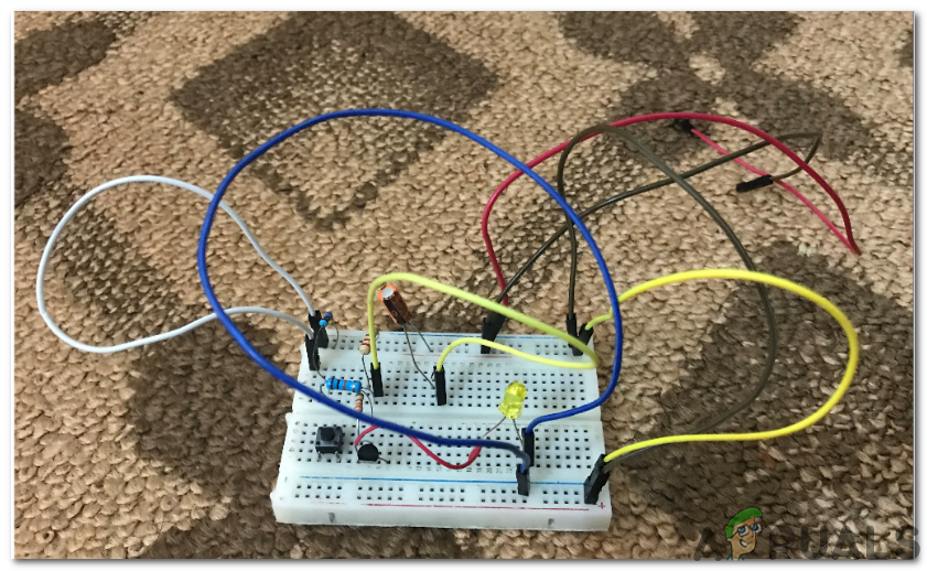
Step 8: Setting Up The Hardware
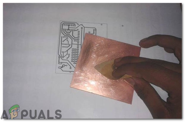
As we have now simulated the circuit on software and it is working perfectly fine. Now let us move ahead and place the components on PCB. A PCB is a printed circuit board. It is a board fully coated with copper on one side and fully insulating from the other side. Making the circuit on the PCB is comparatively a lengthy process. After the circuit is simulated on the software, and its PCB layout is made, the circuit layout is printed on a butter paper. Before placing the butter paper on the PCB board use the PCB scrapper to rub the board so that the copper layer on board is diminished from top of the board.
Then the butter paper is placed on the PCB board and ironed until the circuit is printed on the board (It takes approximately five minutes).

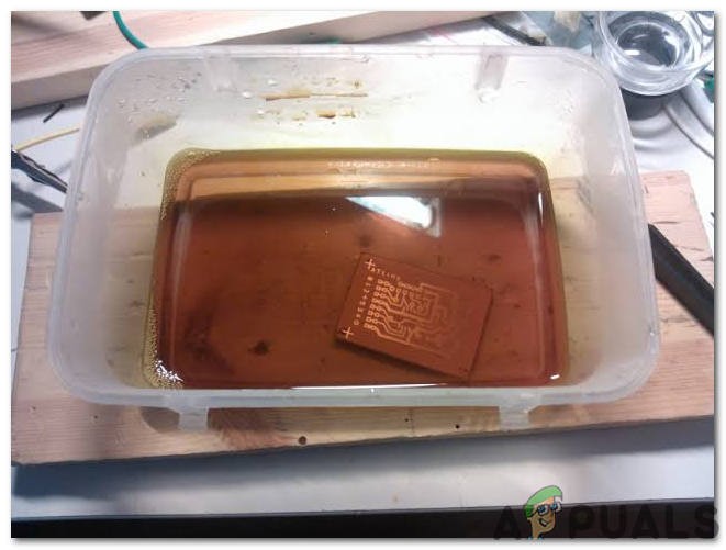
Now, when the circuit is printed on the board, it is dipped into the FeCl3 solution of hot water to remove extra copper from the board, only the copper under the printed circuit will be left behind.
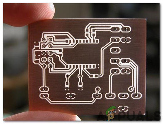
After that rub the PCB board with the scrapper so the wiring will be prominent. Now drill the holes in the respective places and place the components on the circuit board.
Solder the components on the board. Finally, check the continuity of the circuit and if discontinuity occurs at any place de-solder the components and connect them again. It is better to apply hot glue using a hot glue gun on the positive and negative terminals of battery so that the terminals of battery may not be detached from the circuit.
Step 9: Testing The Circuit
After assembling the hardware components on the PCB board and checking the continuity we need to check whether our circuit is working properly or not.
- Switch On The Circuit.
- On pressing the push button we will observe that LED fades up.
- The capacitor that is connected to the resistor in parallel starts charging and during this charging process, some voltage is given to the base of the transistor which then starts the conduction process.
- The emitter is connected to the ground in the circuit and during the charging process, some voltage is provided to the emitter which is connected to the ground.
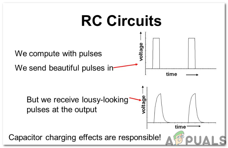
- As the LED is connected to the ground and it starts glowing and capacitor produces the square pulses which are shown below:
Capacitor Charging - The capacitor starts discharging when the push button has released the capacitor discharging process is started hence, the LED starts fading out.
- A resistor is placed before BC 548 transistor so that the capacitor discharges through this resistor.
Applications
- A little transformation will be needed in this circuit and it can be installed in the parking lot and the lights present there will turn automatically ON and OFF.
- This prototype can be used by the security companies to show an alert situation.
- It can be placed in shopping malls to turn OFF the lights hence, saving energy in the area where there are no people present.